As a business leader, one might scoff at the thought of inspiration in leadership. Some business leaders may dismiss the vision as over-the-top, and perhaps even pretentious. But, the world of innovation, creating wealth, great professional bonds can all be a little jarring. Without inspiration to drive a natural sense of curiosity and aspiration – the rail of productivity can quickly lose steam. On the other hand, there is a concrete way to step forward, to build, and to deliver inspiration. A company that encapsulates the spirit of inspiration at every step is NEO Semiconductor.
A Game-Changing Innovation
Soon after its beginning in San Jose, California in 2012, the company dedicated in 3D NAND flash memory technology and, after six years of development, devised its signature X-NAND architecture for semiconductor chips. The architecture has become a benchmark for excellence in the semiconductor industry. The award-winning architecture solves the key issue of speed and lack of adaptation in old semiconductor chips. Today, the X-NAND architecture improves random read and write speeds by 3 times, sequential write speeds by 15 times, and sequential read speeds by 30 times. This is the benchmark of excellence at NEO Semiconductor in a nutshell.
NEO Semiconductor creates solutions to some of the most pressing technology issues of our time. NEO Semiconductor focuses on developing fundamentally game-changing technology. Once it has achieved this goal, it offers the technology to the world at large. Its clients stand to win by applying their IP patents to some remarkable challenges that are at the forefront of commercial investments. However, it isn’t just the commercial promise of its application that makes the company stand out among its competitors.
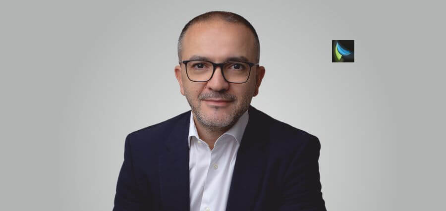
The X-NAND architecture solves the core issue of flexibility and adaptability in semiconductor chips. Major technology giants like Microsoft, Amazon, Google are pushing chip manufacturers to create AI-enabled chips. These chips need to access massive data and AI algorithm stored in high-speed emerging memory chips. These memory chips are likely to be tremendously expensive, and their potential adaptation to millions of upcoming AI function remains a worry. On the other hand, the X-NAND simply offers new architecture to drastically increase the performance of NAND flash memory for single-level cell, multi-level cell, triple-level cell, and quad-level cells. Its adaptation to various different cell levels enables it to offer data storage systems in key futurist applications like AI, IoT, and cloud. According to Andy Hsu, the Founder and CEO of NEO Semiconductor, “the architecture offers a high-speed, high-density, low cost, low risk, fast-turnaround solution for NAND flash memory”.
A Prospect of Stability in Global Supply Chains
The semiconductor industry is on the verge of a major leap in terms of technology. On the one hand, the issues with speed, adaptability, and upcoming AI applications remain key challenges for the semiconductor business. This has resulted in major supply chain delays across the globe, resulting in increased costs and disruptions in cross-industry collaboration. On the other hand, AI applications promise a new arena of opportunities for the semiconductor which transcend beyond some wild theories on commercial prospects. For example, semiconductor chips are likely to be introduced in new automated vehicles, and every other AI-driven future application, including refrigerators, smartphones, IoT, virtual personal assistants, and more. These all rely on high-speed processing of huge amount of data stored in memory chips. However, the technology to make the leap is missing.
NEO Semiconductor’s signature X-NAND architecture promises to solve the on-going supply disruption in the high-speed data storage industry. The supply chain disruption has partially come to the fore due to increased demand from clients to upgrade NAND flash memory. This is critical for the growing need to improve data storage for a wide range of machine learning, and AI applications. However, solving this challenge is not straightforward. For example, while upgrading traditional memory modules to emerging memories like FRAM, PCM, RRAM, requires new processes, and new materials. On the other hand, the X-NAND architecture does not require clients to invest in new technology, and can be directly applied to the old technology. Hence, companies can integrate X-NAND technology in their existing AI-enabled NAND flash memory framework to build the next product without any additional costs, research, or delays.
An Inspirational Journey
In 2020, NEO Semiconductor was awarded the ‘Most Innovative Flash Memory Startup’ Award at the Flash Memory Summit. Its CEO believes NEO Semiconductor will continue to scale new heights, thanks to the growing backbone of its expertise in the 3D flash chip arena. Today, the company is solving a wide range of challenges in the semiconductor industry, including resistive memory, AI chip technology, ultra-low power CMOS-based IoT memory, and phase-change memory. Andy notes that these are key to embracing an increasingly mobile workforce. “As the pandemic raged on, everything in-between working, education, gaming, social interactions became virtual”.
This has sparked a tremendous demand for faster, and higher density NAND flash memory systems”. NEO Semiconductor is ready to tackle the growing challenge of competition head-on with its signature technology. The company plans to offer a customized solution to key business arenas like cloud, and data centers with specialized solutions. NEO Semiconductor will provide TLC-QLC products for data centers, and cloud providers. Moreover, it will offer SLC-MLC products for mid-stream applications such as Storage Class Memory or SCM. For down-stream applications such as embedded systems, the company will offer serial NAND flash memory. The strategic and wise planning will likely ensure a speedy scaling up of entire data storage hierarchical system to meet the needs of most stakeholders in the industry.
Every organization aims to instill an inspired workforce at the heart of its operation. Such operation is critical for the success of most but essential for enterprises investing in breakthrough R&D. Knowledge is often acquired as building blocks to build something bigger, and better. Such acquisition can take years in efforts, and investment. Furthermore, such investments reside in the murky waters of uncertainty. For example, a company seeking to find a replacement for lithium-ion material for electric batteries may never find one. Hence, a company culture geared to find the next big thing in the R&D arena must find ways to inspire itself every day. Some say, inspiration in essence is devotion personified, and the leadership at NEO Semiconductor seems to agree. According to Andy, “The persistence, confidence, and the relentless efforts of my team have inspired our successful journey”.
A Committed Path to Success
Andy Hsu, and the co-founder of NEO Semiconductor, Ray Tsay are witnesses to many technological challenges every day. Ray notes, “We plan to advance semiconductor technology to everyone’s benefit with our IP solutions”. NEO Semiconductor has opted for a unique path to business growth. Nearly every company in the business builds technology to make a fortune for itself. While there is nothing wrong with it, very few understand the trouble that comes with it. Especially for a startup company, it is a huge challenge for market competition. NEO Semiconductor has chosen an off-beat but wise path to growth. The company provides IP to its clients, and remains committed to its core area of research, by sacrificing potential of sales, and the burden of marketing operations among others.
A Precious Investment
In recent years, NEO Semiconductor has taken effort to the media lane to inform the public about its breakthrough technology. Since its inception, the company has walked a clear path to work behind closed doors, and remain stoic in pursuit of innovation. However, in its effort to give back to the community, the company plans to invest in education of science and technology in various ways. The company founders now frequently attend conferences, media events, and virtual seminars to spread positivity about innovation in science and technology., NEO Semiconductor has been scheduled to be featured on CNBC Advancement TV series educational program. The program will go on air in November 2021.
Only time can tell whether company’s investment in education pays off. However, with a committed and devoted team effort, there is very little to stop NEO Semiconductor to reach the pinnacle of success.


